عضویت
عضویت  ورود اعضا
 راهنمای خرید


Ultra Fast Response Rectifier Diodes CD1408-FU1xx0 pages
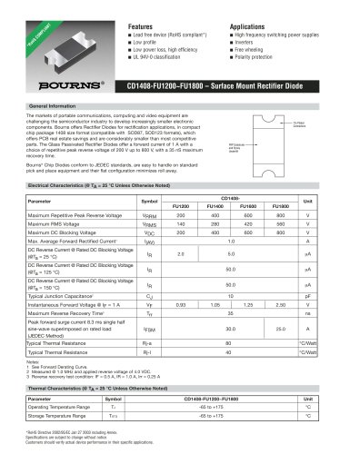
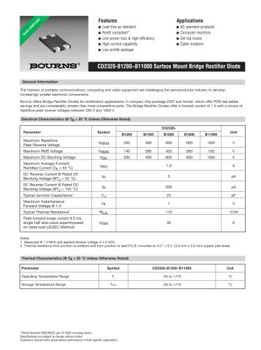
CD1408-FU1200~FU1800 – Surface Mount Rectifier Diode
*RoHS Directive 2002/95/EC Jan 27 2003 including Annex.
Specifications are subject to change without notice.
Customers should verify actual device performance in their specific applications.
Features
¡ Lead free device (RoHS compliant*)
¡ Low profile
¡ Low power loss, high efficiency
¡ UL 94V-0 classification
Applications
¡ High frequency switching power supplies
¡ Inverters
¡ Free wheeling
¡ Polarity protection
General Information
The markets of portable communications, computing and video equipment are
challenging the semiconductor industry to develop increasingly smaller electronic
components. Bourns offers Rectifier Diodes for rectification applications, in compact
chip package 1408 size format (compatible with SOD87, SOD123 formats), which
offers PCB real estate savings and are considerably smaller than most competitive
parts. The Glass Passivated Rectifier Diodes offer a forward current of 1 A with a
choice of repetitive peak reverse voltage of 200 V up to 800 V, with a 35 nS maximum
recovery time.
Bourns® Chip Diodes conform to JEDEC standards, are easy to handle on standard
pick and place equipment and their flat configuration minimizes roll away.
*RoHS COMPLIANT
Tin Plated
Connectors
FRP Substrate
and Epoxy
Underfill
Electrical Characteristics (@ TA = 25 °C Unless Otherwise Noted)
Thermal Characteristics (@ TA = 25 °C Unless Otherwise Noted)
Parameter Symbol CD1408-FU1200~FU1800 Unit
Operating Temperature Range TJ -65 to +175 °C
Storage Temperature Range TSTG -65 to +175 °C
Parameter Symbol
CD1408-
Unit
FU1200 FU1400 FU1600 FU1800
Maximum Repetitive Peak Reverse Voltage VRRM 200 400 600 800 V
Maximum RMS Voltage VRMS 140 280 420 560 V
Maximum DC Blocking Voltage VDC 200 400 600 800 V
Max. Average Forward Rectified Current1 I(AV) 1.0 A
DC Reverse Current @ Rated DC Blocking Voltage
(@Ta = 25 °C)
IR 2.0 5.0 ìA
DC Reverse Current @ Rated DC Blocking Voltage
(@Ta = 125 °C)
IR 50.0 ìA
DC Reverse Current @ Rated DC Blocking Voltage
(@Ta = 150 °C)
IR 50.0 ìA
Typical Junction Capacitance2 CJ 10 pF
Instantaneous Forward Voltage @ IF = 1 A VF 0.93 1.05 1.25 2.50 V
Maximum Reverse Recovery Time3 Trr 35 ns
Peak forward surge current 8.3 ms single half
sine-wave superimposed on rated load IFSM 30.0 25.0 A
(JEDEC Method)
Typical Thermal Resistance Rj-a 80 °C/Watt
Typical Thermal Resistance Rj-l 40 °C/Watt
Notes:
1 See Forward Derating Curve.
2 Measured @ 1.0 MHz and applied reverse voltage of 4.0 VDC.
3 Reverse recovery test condition: IF = 0.5 A, IR = 1.0 A, Irr = 0.25 A