عضویت
عضویت  ورود اعضا
 راهنمای خرید


SIPLACE CA0 pages
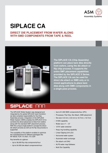
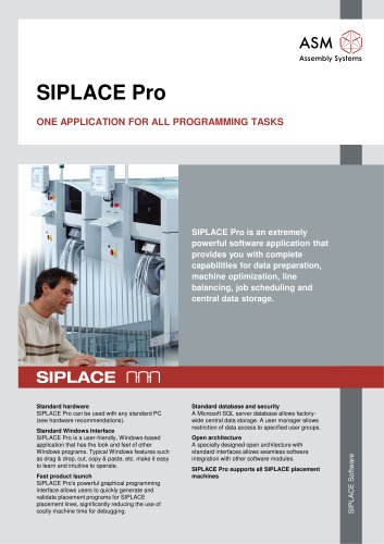
SIPLACE CA
DIRECT DIE PLACEMENT FROM WAFER ALONG
WITH SMD COMPONENTS FROM TAPE & REEL
The SIPLACE CA (Chip Assembly)
platform can place bare dies directly
from wafers, using the die attach or
flip chip process. It supports the
entire SMT placement capabilities
provided by the SIPLACE X Series.
The SIPLACE CA can be used for
direct die attach or SMD only or in
mixed applications to place bare
dies along with SMD components in
a single pass process.
Up to 81,000 SMD components/hour (IPC)
Processes: Flip Chip, Die Attach, SMD placement
Die size: 0.8 mm x 0.8 mm to 18.7mm x 18.7mm
01005 capability
Wafer size: 4" – 12"
12"/8“ wafer stretcher
Hoop ring handling capability
The scalability of the platform enables to optimize
the cost/placement for different packages like
RF-MCM, FCIP, FC-MLF, FC-CSP.
Linear Dipping Unit LDU
Horizontal wafer system
Automatic wafer exchange
Die attach unit DAU
ALPS wafer map Software
Multi Die Capability
Key benefits at a glance:
Up to 36,000 flip chip components/hour
Up to 24,000 die attach components/hour
SIPLACE Hardware
The SIPLACE Wafer System was designed and
integrated by the global SIPLACE team therefore
we take complete responsibility for the Chip
Assembly process. Integration of the SIPLACE
Wafer System (SWS) enables the SIPLACE CA to
combine the direct placement of dies from wafers
along with the standard SMT placement process.
With this unique single platform concept the direct
die attach process as well as the flip chip process is
supported.